|
Part
the third. Detailed. For those who not bad understands
and wants to understand all subtleties.
Evolution Slot1-PPGA-FCPGA-FCPGA2.
To understand "radically" we shall look
at a problem "globally" - we shall consider
a way of development of P6-processors Slot1/PPGA/FCPGA/FCPGA2.
Last from a ruler was FCPGA2 Pentium III-S Tualatin
(L2=512kB, 1466MHz max)? Therefore all we shall compare
to it since he, understandably, has the greatest quantity
of the involved conclusions (i.e. in him is simply
"Reserved" legs).
To not overload the given material unnecessary "statistics"
(numerous identical to all processors signals), I
shall result only those legs / signals which varied
during development ruler of P6-processors:
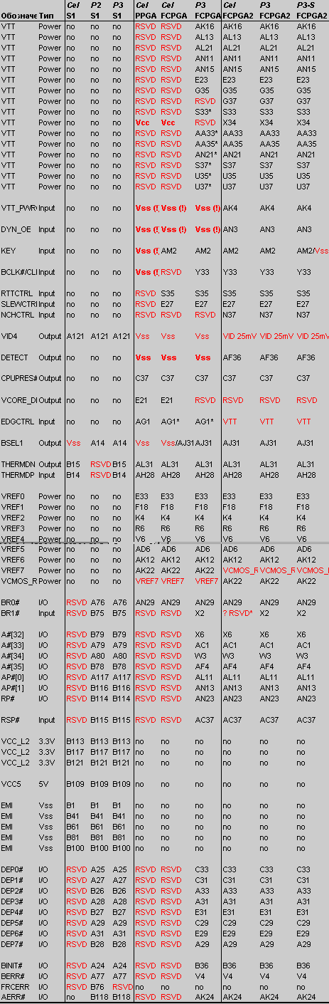
It is a lot of touching various variants of a statement
of the information has finally got confused, therefore
simply "mechanically", under the order of
following in the table, I shall stop on everyone.
Vtt - a voltage termination (AB36, AD36, AG1,
AH20, AK16, AL13, AL21, AN11, AN15, E23, G35, G37,
S33, X34, AA33, AA35, AN21, S37, U35, U37).
At once the most numerous group - signals Vtt is evident.
For slotked processors of them only four therefore
as further she (termination) is dissolved already
on the cartridge of the processor. We shall stop in
more detail on running terms - "termination",
" a voltage of termination ".
As is known, bus GTL + (Gunning Transceiver Logic),
however, as well as AGTL +/AGTL, as against the previous
processors using for signals TTL-logic, is constructed
basically on structures with an open drain (open drain)
which for reduction of the reflected signals should
be named on both ends of each alarm line. "Are
named" - means are connected through the resistor
to the certain high level (+1.5V for AGTL + and +1.25V
for AGTL) which is the maximal value logic "1".
All signal inputs are differential and use a basic
voltage (V_REF), equal 2/3 from Vtt. At a level smaller,
than (V_REF-0.2V) the signal is perceived as "0",
at a level the greater, than (V_REF+0.2V) - as "1".
Dependence and "0" and "1" only
from one value Vtt allows to get on safely to such
bus on the different nucleus made on different technologies
and, the main thing, having a various voltage of a
power.
In case of uniprocessor system on one end of an signal
line the chipset, on another - the processor settles
down. Accordingly, one the resistor of termination
should be located as it is possible closer to a chipset,
another - to the processor.
In slotked processors they (resistors of termination)
settle down on a cartridge.
In case Celeron-Mendocino - they should be or close
PPGA-connector, or on adapter Slot1-> Socket370.
Since FCPGA-processors all termination has been integrated
already inside of the processor (on die) and consequently
demands only submission of voltage Vtt on corresponding
contacts (see tab.).
VttPWRGD - VttPowerGood (AK4).
The signal has appeared in Tualatin. Because of similarity
with "PowerGood" the some people it is accepted
for " a voltage of termination signal PowerGood
", that, to put it mildly, it is far from true.
In a reality all is essentially more difficult and
easier simultaneously.
Why it is more difficult? It is difficult to understand
why the signal everywhere marked as Input only at
it in datasheet on all Tualatin has precise:
"The VTT_PWRGD signal informs
the system that the VID/BSEL signals are in their
correct logic state. During Power-up, the VID signals
will be in a indeterminate state for a small period
of time. The voltage regulator or the VRM should not
sample and/or latch the VID signals until the
VTT_PWRGD signal is asserted. The assertion
of the VTT_PWRGD signal indicates the VID signals
are stable and are driven to the final state by the
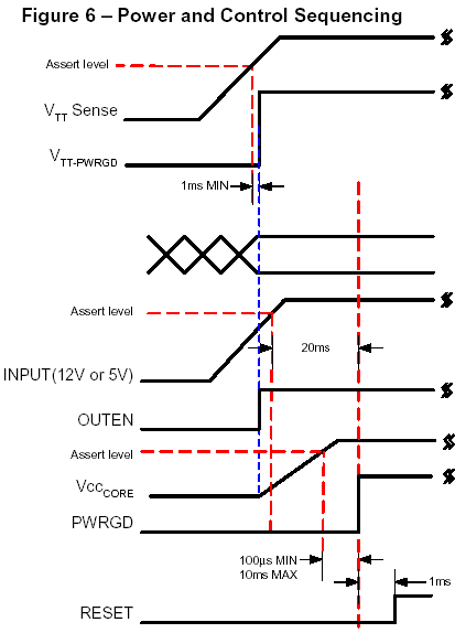
processor. Refer to Figure 6 for power-up timing sequence
for the VTT_PWRGD and the VID signals".
I.e. Signal Vtt_PWRGD speaks system that signals
VID/BSEL are already exposed in the nominal status.
Simply, as against Slot1/PPGA/FCPGA-processors, at
Tualatin these legs (BSEL0/1, VID0-4) are not set
"analog" (i.e. it is simple or "shorted"
on the ground inside the processor for "0",
or are left " Not Connected " for "1"),
and cope the processor which exposes on them necessary
"combination". It has been
made, probably, counting upon an opportunity of program
management by a voltage of a power and as, that is
more probable:), complicating to us remaking of old
motherboards under Tualatin (drawn for itself conclusions
after similar process PPGA-> FCPGA).
From the description it is possible to draw a conclusion,
that Vtt_PWRGD very much even "target",
instead of "entrance". In fact even the
same VRM it should, type "wait": "VRM
should not... ...until the VTT_PWRGD...".
But we not begin to give in to this muffled and even
to the inconsistent description - we shall look at
description VttPWRGD from datasheet on VRM8.5. There
with all severity it is said, that he (VttPWRGD) nevertheless
"input" (for the processor), as "day
off" for him (VRM-a):
"VTT_PWRGD is an active HIGH signal used to
indicate to the processor and to the clock
generator that the processor VTT plane is above the
minimum specified level of 1.14V."
I.e. VTT_PWRGD informs the processor (and the generator,
by the way) that voltage Vtt has achieved a minimum
level of logic unit. (And legs of the name - "
Power Good for Vtt " from here grow.)
All begins on the places if to take into account,
signal VttPWRGD (as well as DYN_OE) is a part of a
circuit for generation Vcc of the processor which
works before start of the processor and this circuit
DYN_OE-> VttPWRGD works, as soon as Vtt will achieve
the minimal value. Logic "1" on DYN_OE allows
to expose on VID/BSEL serves, actually (excuse for
tautology) for his start. The necessary combination,
and on VttPWRGD she ("1") should appear
with a delay thanking VRM (instead of to the processor!).
The delay (~1mS) is entered avoiding reading of combination
VID/BSEL, while they in a "transitive" status.
And reading VID/BSEL begins only after VttPWRGD becomes
equal "1", i.e., as a matter of fact - with
a banal delay 1mS which VRM generates " for itself
" (instead of for the processor). For the processor
"important" only presence "1"
(on VttPWRGD), as acknowledging about stability Vtt
(instead of mentioned in description VID/BSEL).
For specification as it is generated VttPWRGD, it
is possible to look at the circuit:
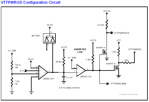
It is visible, that "1" on him will appear
only after stabilization of the basic voltage.
For visual performance when there is signal VttPWRGD:
The unsigned schedule (enemies - everywhere confuse;)
- it is obvious levels VID/BSEL.
More shortly, the main conclusion - VttPWRGD has
no any relation к PWRGOOD, therefore to connect
them (AK4 and AK26) it is not necessary. Besides
- it is impossible, for it is dangerous,
since levels at them differ twice! VttPWRGD should
be 1.25V, and PWRGOOD in old motherboards it is connected
to 2.5V for this reason VttPWRGD it is necessary
to connect with с Vtt. More precisely - it is
possible "to connect" only in a case when
in the same remaked jack it will not be stuck
stuck "non Tualatin" the processor if it
is supposed "universal" a socket - it
is necessary to connect through 0.1-1kOm the
resistor since in old processors this conclusion sits
on the ground and can burn out in a case of the "direct"
application to him Vtt.
DYN_OE - Dynamic Output Enable (AN3).
Сигнал появился в туалатинах. Как упомяналось чуть
выше - разрешает установку уровней VID/BSEL. Никакой
больше особой "нагрузки" не несёт и побольшому
счёту, DYN_OE представляется собой лишь одну из нескольких
банальных "защит от переделки" (или говоря
официальным языком - "предотвращение установки
туалатина в неподдерживающую его платформу";)
The signal has appeared in Tualatin. As mentioned
hardly is higher - resolves installation of levels
VID/BSEL. Special "loading" any more does
not bear and DYN_OE it is represented only one of
several banal " protection against remaking "
(or speaking an official language - " prevention
of installation Tualatin in a platform not supporting
it ";)
Active level - logic "1" which appears on
him at achieved Vtt level V_REF at once after inclusion
even before submission Vcc. This signal, as well as
VttPWRGD - part VRM8.5, transferred in the processor
(therefore also works up to and for
his start).
At remaking it is isolated. There is some lack at
" simply isolation " (without factory Vtt
- as for VttPRWGD). Initially a signal on the ground,
therefore, certainly, we also isolate it, but what
level of a voltage thus will appear on becoming "NotConnected"
contact - depends on concrete mother and a concrete
copy of the processor. Usually there appears "1"
(through internal circuits), however I not time met,
when, probably, "1" had an insufficient
level therefore VID + BSEL remained in position 1/1/1/1/1
+ 1/1. VID4 at remaking under Tualatin becomes isolated
on the ground ("0") that gives us "on
- default" - 0/1/1/1/1=1.3V and 1/1=133MHzFSB.
Seldom what Tualatin start on the increased frequency
at the underestimated voltage so be attentive and
necessarily check - what voltage "exposes"
the processor!
The decision of such problem can shorted "necessary"
VID/BSEL on the ground be similar VID4. However here
there can be already other problem - how to be spoken
- " was ill from by what it was treated ".
Having closed "compulsorily" on the ground,
for example, 0/0/1/1/1=1.7V (for example, for overclocking)
and then having established in the same motherboard
other processor (even precisely same face value, but
it is simple - another) - can be received not 1.7V,
and 1.9V = 0/0/0/1/1. Simply that "will suffice"
other copy "simiunity" on DYN_OE and he
will fairly expose a "additional" zero on
VID2. In addition I shall say, that, everything, such
("floating" levels VID/BSEL because of DYN_OE)
happens not too often, but - happen. So be not lazy
to use voltmeter before to fall asleep forums messages
about next "glitching" to an adapter / motherboards,
etc.
As the conclusion from this point - for alteration
under Tualatin AN3 is subject to isolation with check
of level Vcc. " True aesthetes " should
apply effort and repeat a feat similar to leg VttPWRGD
- isolation from the ground at submission on it Vtt.
Key - AM2.
The signal has ceased to be "ground" in
Coppermine. Together with VttPWRGD/DYN_OE for Tualatin
and AH4 for Coppermine, represents only one of "
protection against remaking ". In Mednicino he
(AM2) earthed, and in Coppermine there is banal have
started RESET# which thus is not used in any way
(i.e. motherboard he is not necessary). In any
way, except for as "key" - whence and the
name.
For remaking under Coppermine - it is banal it is
isolated. In case of remaking PPGA under Tualatin,
it is natural - too it (is isolated).
By the way, in CPU P3-S/Tualatin (L2-512kB) he (AM2)
- already NotConnected, and on motherboards "special
for him" (server dual-systems) AM2 - on "ground"
that it was impossible to put "usual", "not
server" P3-Tualatin. Simply song;)
BCLK#/CLK_REF - Bus Clock / Clock Referency Voltage
(Y33).
In CPU Pentium III Coppermine was one interesting
innovation concerning clocking of the processor -
he could synchronized not only from one "unipolar"
clock pulse BCLK, and also from his "doubled"
analogue - pairs BCLK/BCLK#:
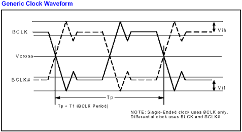
It has been made (" Differential Clock "
instead of "Single-Ended") for improvement
of stability (exception of cross handicapes - they
mutual compensation at subtraction BCLK - BCLK#).
That "kindness" of Intel which is expressed
that the processor itself determines a way
of clocking, by the way, is not absolutely clear,
i.e. can use both kinds (and "
Differential Clock " и "Single-Ended")
synchronization (i.e. why made so much artful "protection",
and it have not touched). At what this opportunity
(auto detection such as synchronization) has remained
even in Tualatin, what it is absolutely strange.
With the advent of processors on nucleus Tualatin
the given signal many for some reason have interpreted
as " basic difference " Tualatin - use of
"double" synchronization, having forgotten
even about that he already was in P3-Coppermine. For
subject to this noxious influence (unfortunately -
iXBT.com here was one of main "powdered":)
I bring endurance{quotation} from datasheet:
I.e. the processor chooses type of synchronization
proceeding from a signal on Y33. If there a constant
voltage (should be 1.25V) synchronization - on forward
front is used "usual" "Single-Ended".
Otherwise - " Differential Clock ", i.e.
pair BCLK/BCLK * is used. Naturally, on old chipsets
is only BCLK, therefore Tualatin (P3-Coppermine) it
will simply safely be switched in "Single-Ended"
a mode and it will be completely quiet and correct
to work.
In case of remaking under Tualatin initially only
Coppermine support a motherboard (adapter) of anything
with contact Y33 to do it is not necessary - there
already should be 1.25V. In a case of remaking PPGA->
FCPGA2 (and even PPGA-> FCPGA) there can be following
subtleties. In PPGA - Y33 on "ground", and
" should be " - +1.25V. I.e. as though once
again it is necessary to repeat the difficult operation
similar VttPWRGD - to isolate from a socket, having
submitted thus a voltage. However practice has shown,
that in most cases the ground on Y33 instead of put
+1.25 does not prevent to work completely safely to
the processor (both P3-Coppermine and P3/Celeron-Tualatin).
Why? - it is difficult to say, probably - " porridge
butter ":) to spoil difficultly (high level BCLK
in relation to CLK_REF). However, nevertheless - it
is possible. Also it is noticed such, for some reason
only basically on motherboards (Slot1) from Gigabyte
and Abit, at what only in ATX-execution.
So, a short conclusion from this point: Y33 we let
alone before final check (it is done other remakings).
And only, if all other remakings are precisely correctly
made (and as in a case Gigabyte-Abit origins of motherboard)
- it it is necessary apply effort with Y33. Recommendations
Intel concerning a divider on Y33 the following:
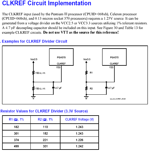
I.e. it is the easiest to take two 150 Ohm resistors
and to get them on 2.5V (" true aesthete "
can put also the condenser specified on the circuit;).
However, even despite of the terrible warning "
about inadmissibility of use Vtt in quality CLK_REF",
in view of safe job in many cases and at earthed Y33
- without ceremony it is possible to try even such
variant (to close Y33 on Vtt). But, nevertheless,
certainly, urgently recommend though through any resistor
(0.1-1kOm).
"To " true aesthetes ", I shall be
repeated, I recommend to not experiment, and at once
to get 1.25V on Y33 (and for remaking under Tualatin
and for installation P3-Coppermine on remaked PPGA).
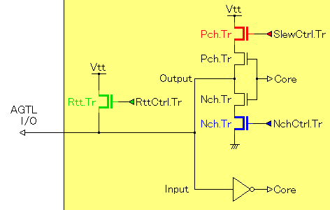
RttCTRL (S35).
(has appeared, since FCPGA).
Rtt Control - sets size of resistance internal resistors
of termination. It is adjusted by shunting of leg
S35 on the ground through the resistor. Than resistance
of "shunt" less - that smaller resistance
will have internal resistors of termination. For platforms
with support Mendocino recommended Intel value - 110
Om, without support (i.e. it is not necessary "to
be arranged" under not having internal termination
processors) - 56 Om, just is so much, how much it
is necessary for standard onboard termination.
From this it is possible to draw a conclusion, that
the processor "reads out" size of resistance
on leg S35 and expose same "at itself
inside ". To what these reasonings? Yes it is
simple from them follows, that if S35 will be "NotConnected"
(as it takes place in PPGA) internal termination it
will be switched - off in general and the processor
will "use" only external - located on parent
a motherboard / adapter. That to us, actually also
it is necessary - on PPGA always is "external"
termination, therefore the FCPGA/FCPGA2-processor
for the lack of resistance on S35 will switch off
internal termination and will work completely safely.
Though, nobody forbids to true "aesthetes";)
to hang up on S35 R~100-200 the Ohm (or 110 as recommends
Intel).
In case FCPGA, S35 according to "recommendations"
already hangs through 110 Om. In case of installation
Tualatin here, understandably, already anything to
touch it is not necessary (and as it was spoken above
- not important).
SlewCTRL (E27).
(has appeared in FCPGA2).
Slew Control - adjusts a steepness
of signals AGTL of the +/AGTL-bus. As well as RttCTRL
it is "only input signal for the processor and
as it is set by size of the resistor on the ground
(on default - the same 110 Om).
Both for Tualatin and for Coppermine platforms Intel
recommends identical value - 110 Om for the ground.
Accordingly, for FCPGA-motherboards this signal it
is ok. In PPGA this signal - "NotConnected".
However already inside the processor he has resistance
about ~300 Om (and, by the way, it same, as well as
for RttCTRL). Therefore, probably, in case PPGA of
it quite suffices - in any case of any changes (though
somehow reflected at job of the processor in various
modes) at change of value this parameter in a course
of our experiments it has not been noticed. And numerous
experience altered confirms it - SlewCTRL at remaking
" it is possible to not take into account ".
Though, besides, " true aesthetes " always
can shorted it on the ground through 110 Om.
(p.s. Who owns more detailed information on this
signal - I shall be mailto:bios@rom.by)
NchCTRL (N37).
(has appeared in FCPGA2).
N-channel Control. From datasheet:
The NCHCTRL input signal provides AGTL pull-down
strength control. The Intel® Pentium® III processor
with 512KB L2 Cache samples this input to determine
the N-channel device strength for pull-down when it
is the driving agent. This signal must be connected
to a 14ohm resistor to VTT. Refer to the platform
design guide for implementation detail and resistor
tolerance.
One of artful and yet up to the end understandable
to me signals. Proceeding from the name it is possible
to assume, that he is intended for management current
by loading of receivers of a signal and it is possible
(necessary) to consider in pair with Slew Control.
In this occasion I shall result some reasons from
N-yagi PC ManiaX (which I too share). He assumes
following conditional " the circuit of inclusion
" signals RttCTRL/SlewCTRL/NchCTRL:
By the way, it is necessary to take into account
"subtlety" of fine tunings with help SlewCTRL/NchCTRL
- she will not be shown in any way in "usual"
system, what not time has been tried (submission on
them the grounds Vtt/Vcc did not allow any obvious
changes). Therefore it is possible to assume influence
of these adjustments only in the dispersed computers
(or DUAL-systems) at what if the above-stated circuit
is correct for the best stability SlewCTRL it is necessary
to leave NotConnected, and NchCTRL to short-circuit
"directly" (without the resistor) with Vtt.
My personal experience and responses of some other
skilled "experimenters" confirm it (SlewCTRL
- NC, NchCTRL - to Vtt) practically.
And more it is possible to add, that leg N37 in the
processor "is initially called" on Vtt through
~450 Om (only - in Tualatin, in Coppermine/Mednocino
- no). Therefore, probably, even if to not apply any
additional actions (since in PPGA/FCPGA she "NotConnected")
it (450 Om to Vtt) quite suffices.
(p.s. Who owns more detailed information on this
signal - I shall be mailto:bios@rom.by)
VID4 (VID 25mV в FCPGA2)
Initially (Slot1) the "five-specific" system
of the task of a voltage of the processor has been
accepted. Simply the first Pentium II had a power
2.8V though fast transition to a power 2V was assumed
and is lower (i.e. the range 1.3-3.5V was "too
wide for use only four VID). Since Pentium II Deshutes
(Celeron Covigton) processors began to have Vcc 2V
and is lower, for which task "sufficed"
only four VID (grown-up VID4 should be always "0"
- the ground). As a result of it VID4 in datasheet
not mentinioned also passed with designation Vss -
the "lifelong" ground.
However it is real on the majority of motherboards
VID4 in a socket not grounded and went direct on the
PWM-CONTROLLER, i.e. it was safely used, that allowed
to expose a voltage 2.1V and is higher. (Therefore
I everywhere "position" it as VID4, a specifying
range of voltage: "0" - 1.3-2.05V, "1"
- 2.1-3.5V).
With occurrence VRM8.5 (FCPGA2) to him gave function
of a 0.25V-adding conclusion - in a case "1"
on VID4 to a "standard" VRM8.4-voltage it
is added 25mV (whence and the name). Therefore in
case of remaking under Tualatin with Vcc=1.475V it
is necessary to be cautious - 1.475V/VRM8.5=2.3V/VRM8.4
(see the table in the second part of article)! Therefore
VID4 it is necessary to ground (though, do not experience
- short-term submission 2.3V will not kill the processor,
is checked repeatedly up;).
Detect (AF36).
(has appeared in FCPGA2).
If to believe datasheet - "cleanly" target
signal. That, basically and logically enough - he
is used "Tualatin" by chipsets (i815EPB/VIA694T)
for determinine of what level to expose for Vtt -
1.25V or 1.5V. In non Tualatin processors this leg
sits on the ground, and in Tualatin - Not Connected,
that is simply caught with the help of a key in VRM8.5.
And now about why I have written " if to believe
datasheet ". The matter is that mysterious influence
AF36 on remaked under Tualatin adapters though it
does not match in any way "sense" and "
only day off " function of a leg was revealed.
On idea, she (AF36) is necessary ONLY for a chipset
(more precisely power unit - for identification 1.25V/1.5V
Vtt). However in some rare cases of remaking PPGA->
FCPGA2 without its removal the processor to start
refused (the truth, at downturn Vcc up to 1.3-1.4V
it was for some reason started). In all cases known
to me it there were adapters PPGA-> FCPGA2 and
motherboards from Asus (such as P2-99). Therefore
in case of such combination (and also - " for
aesthetes ":) I can recommend to remove this
leg - becomes exact not worse:) (though does not any
make "in addition", if the processor was
started).
p.s. see Part4 for some comments about this signal...
CPUPRES# (C37) - CPU Present - a signal of
"presence" of the processor. It is used
motherboard (together with signals from VID's) for
definition, whether the processor (or it is special
"terminator" for "dual" systems
FCPGA/FCPGA2 at one processor) is inserted. In "usual"
(i.e. "not - dual"), as a rule, it is not
used absolutely.
Vcore_DET (E21).
Definition of a voltage of a nucleus.
Additional, "cleanly" target signal. It
is used by some chipsets (for example, i815_A0-step
- GMCH/SM_MAA9) for additional adjustment depending
on processor Coppermine / non Coppermine. In case
Mendocino, on him (E21) it turns out "1",
Coppemine - "0". In Tualatin - it is not
used any more. What that "influences" has
not been noticed was not, though, besides, "
true aesthetes " in a case Tualatin on i815A0
can grounded it in addition.
EDGCTRL (AG1) - "is "clean"
PPGA's a input signal, proceeding from the description
it is used for the task of a level target buffers
(The EDGCTRL input adjusts the edge rate of AGTL+
output buffers and should be pulled up to VCCCORE
with a 51±5% resistor. NOTE: This signal is NOT used
on the FC-PGA package.)
There are some suspicions ("only" IMHO),
that in FCPGA/FCPGA2 he "was divided" on
SlewCTRL/NchCTRL.
(p.s. Who owns more detailed information on this signal
- I shall be mailto:bios@rom.by)
BSEL1 (AJ31).
Bus Select - a choice of frequency of the system
bus.
In processors with FSB 66MHz it was not used (sits
on the ground), for a setting 100/133MHz on him should
be "1".
FSB MHz - BSEL1/BSEL0: 66 - 0/0, 100 - 1/0,
133 - 1/1.
ThermDN/ThermDP (AL31/AH28).
The cathode and the anode built - in thermodiodes.
It was not only in most "pioneer" Pentium
II (Klamath - 233-333MHz). Allows to supervise temperature
of a nucleus of the processor. However "absolute"
accuracy of it is low (~ 7 degrees, therefore infinite
reasonings in various forums"... At me has shown
so much degrees, and at you? " - simply naive
phrasemonger) and to take into account is possible
only really exact "relative" changes.
Vref1, Vref2, Vref3, Vref4, Vref5, Vref6, Vref7
(VCMOS_REF).
Basic voltage for definition "0" / "1"
on trunk AGTL. It is equaled 2/3 from Vtt.
In FCPGA2 Vref7 "began" VCMOS_REF
REF and serves as a basic signal for definition "0"
/ "1" signals of a CMOS-level (non-AGTL).
Simply in non Tualatin processors both V_CMOS
and Vtt were identical (1.5V), and in Tualatin
they (V_CMOS and Vtt) already, naturally,
differ (1.25V and 1.5V).
BR0/BR1.
BREQ0/BREQ1 - Bus Request.
A32, A33, A34, A35.
Four senior address lines - for ECC-correction. Are
absent at all Celeron processors, except for Tualatin's.
AP1, AP2.
Address Parity - " paritet signals "
- , Request Parity, Responce Parity.
Are absent at all Celeron's, except for Tualatin's.
RP, RSP.
Vcc_L2 - a voltage of a L2-cache. The reason
of absence in S370 - L2-cache now it is built - in
the processor.
Vcc_5 - voltage +5V. The reason of absence
in S370 - it was necessary only for formation of signals
on a cartridge of the Slot1-processor.
EMI - e same ground, only with claims for
reduction of electromagnetic radiation (therefore
settles down in regular intervals on all length Slot1).
DEP1, DEP2, DEP3, DEP4, DEP5, DEP6, DEP7.
DEP - Data ECC Protection.
ECC-signals, are used at the established ECC-memory,
are absent at all Celeron's, except for Tualatin's.
BINIT.
FRCERR (B76) - FRC Error - exotic, it is extreme
Slot1-"dual", a PentiumII-signal (in PentiumIII-Slot1
and Celeron-Slot1 - is absent). It was applied in
systems of the extremely critical to integrity of
the data where two processors are used as one, is
more exact - pair: one master, another - slave and
the second only supervises "correctness"
of all operations. In general, something such as RAID
in case of his use as "mirrors" - for greater
reliability of preservation of the information or
job with the data for the processor.
Шина Vtt.
Because of carry of all termination inside of the
processor (FCPGA/FCPGA2) a plenty of "new"
legs (Vtt) "was required". As a matter of
fact - the new bus (topological) Vtt, except for already
existing Vcc and Vss has appeared. However the most
part of legs Vtt (everything, except for X34 and G37)
in FCPGA/FCPGA2 is primary shorted in the processor,
therefore obligatory distributing recommended Intel
on all legs Vtt (as is - "bus") - "type"
for more stable job. In PPGA only on one contact comes
Vtt=1.5V - AD36 (V_1.5) - and then "creeps away"
on all Vtt-legs in the processor (there is a conversation
about remaked PPGA-> FCPGA/FCPGA2). Despite of
the obvious contradiction with recommendations Intel
(which the condition of supply Vtt to each leg on
a motherboards recommends to observe strictly moreover
and tracks wider), it does not reduce stability for
such remaking - current Vtt is too small (no more
~2A) therefore such influence is minimal.
Well, and as always, to " true aesthetes ",
not experiencing for the spoiled appearance of an
adapter, nothing will prevent to throw manually crosspieces
between Vtt-legs (beginning from AD36) in case of
the remaked PPGA-adapter (on everything, I think,
precisely superfluous - the pair - three quite will
suffice).
Part 1. Part
2. Part 4.
|